D Flip Flop Truth Table
One main use of a D-type flip flop is as a Frequency Divider. The name T flip-flop is termed from the nature of toggling operation.
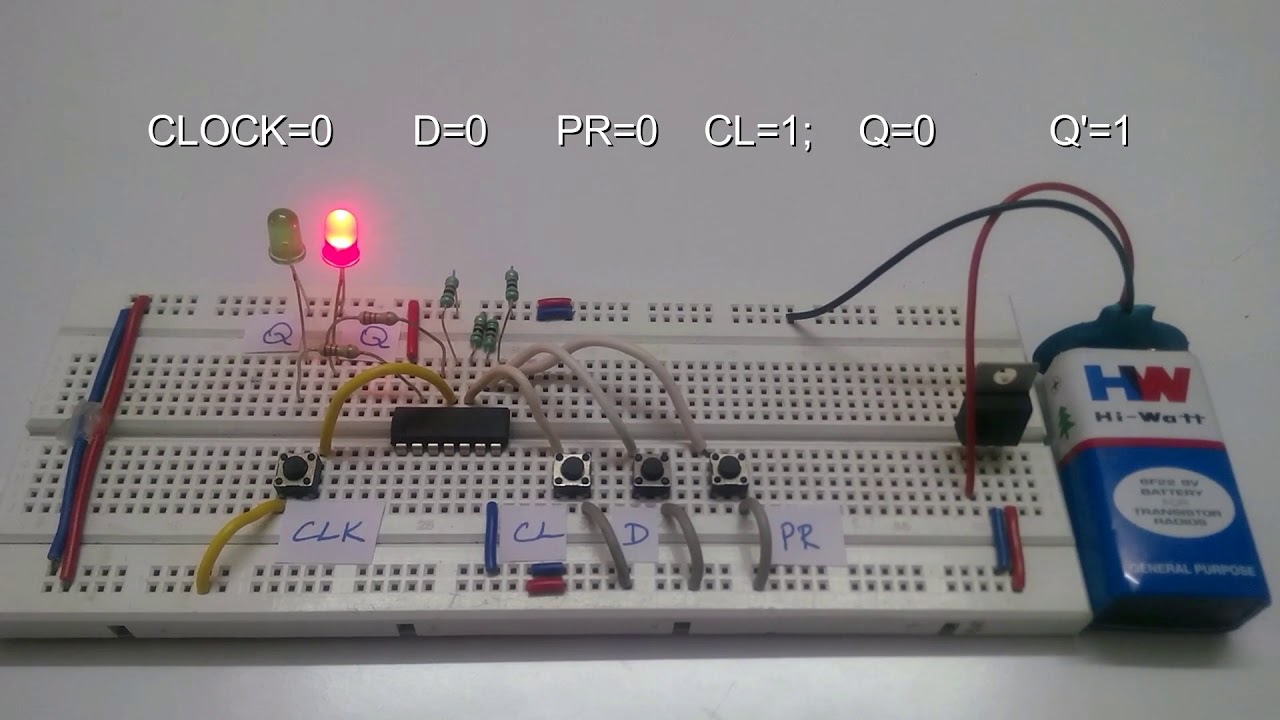
D Flip Flop Circuit Truth Table Working
But now-a-days JK and D flip-flops are used instead due to versatility.

. The Master-Slave Flip-Flop is basically two gated SR flip-flops connected together in a series configuration with the slave having an inverted clock pulse. The CP input is provided. Edge Triggered D flip flop with Preset and Clear.
Behavioral Modeling of D flip flop. Using The D-type Flip Flop For Frequency Division. Here in this article we will discuss about T Flip Flop.
It is the drawback of the SR flip flop. Thus comparing the NAND gate truth table and applying the inputs as given in D flip-flop truth table the output can be analysed. The disadvantage of the D FF is its circuit size which is about twice as large as that of a D latch.
In D flip-flop if D 1 then S 1 and R 0 hence the latch is set on the other hand if D 0 then S 0 and R 1 hence the latch is reset. Power consumption in Flip flop is more as compared to D latch. This is known as a Gated D Latch.
Qp1 simply suggests the future values to be obtained by the JK flip flop after the value of Qp. However the outputs are the same when one tests the circuit. If the Q output on a D-type flip-flop is connected directly to the D input giving the device closed loop feedback successive clock pulses will make the bistable toggle once every two clock cycles.
D Flip-flop Data JK Flip-flop Jack-Kilby T Flip-flop Toggle Out of the above types only JK and D flip-flops are available in the integrated IC form and also used widely in most of the applications. This type of flip-flop is known as a gated D-latch. Consider the circuit shown above.
Inspite of the simple wiring of D type flip-flop JK flip-flop has a toggling. The circuit diagram and truth table is given below. The waveforms pertaining to the same are presented in Figure 3.
The major applications of JK flip-flop are Shift registers storage registers counters and control circuits. During the rest of the clock cycle Q holds the previous value. The name JK flip-flop is termed from the inventor Jack Kilby from texas instruments.
D flip-flop Truth table reset and clock input Asynchronous D flip flop. T Flip Flop. When S 0 R 0 the respective next state outputs will be Q 1 1 and Q 1 1 which is not allowed since both are complement to each other.
At other times the output Q does not change. Now lets make K-map for input D. S D Q N1.
JK Flip Flop Truth Table. JK flip flop is a refined and improved version of the SR flip flop. Thats why delay and.
In this state the output of JK flip-flop will toggle for each positive-edge of the clock signal red lines in the figure. D-latch is a level Triggering device while D Flip Flop is an Edge triggering device. In the counters tutorials we saw how the Data Latch can.
Module dff_behaved clk q qbar. The D flip-flop captures the value of the D-input at a definite portion of the clock cycle such as the rising edge of the clock. The truth table for D flip-flop is as shown in the table.
Lose the control by the input which first goes to 1 and the other input remains 0 by which the resulting state of the latch is controlled. When a triggering clock edge is detected Q D. The table is then completed by writing the values of S and R.
The logic symbol for the D flip-flop is shown in the figure. Here in this article we will discuss about SR Flip Flop and will explore the other Flip Flop in later articles. Consider a positive edge triggered JK flip-flop whose inputs are tied-together and driven high as shown in Figure 6.
From the waveform it is evident that if the input clock period is Tin then the time period of output waveform Tout is twice of it. When D flip-flop generates output independent of the clock signal then the output produced may be asynchronous. Due to its versatility they are available as IC packages.
Table-6 Extended Excitation Table of D And T Flip flop. Operation and truth table. It is a clocked flip flop.
Again starting with the module and the port declarations. That captured value becomes the Q output. If the input R is at logic level 0 R 0 and input S is at logic level 1 S 1 the NAND gate Y has at least one of its inputs at logic 0 therefore its output Q must be at a logic level 1 NAND Gate principles.
The edge triggered flip Flop is also called dynamic triggering flip flop. Moreover it is to be noted that the working of the negative edge-triggered flip-flop is similar to that of positive-edge triggered one except that the changes occur at the trailing. There are many applications where separate S and R inputs not required.
So the two inputs of NAND gate B are R. D flip flop is actually a slight modification of the above explained clocked SR flip-flop. The outputs from Q and Q from the Slave flip-flop are fed back to the inputs of the Master with the outputs of the Master flip flop being connected to the two inputs of the Slave flip.
It stands for Set Reset flip flop. From the figure you can see that the D input is connected to the S input and the complement of the D input is connected to the R input. The truth tables for the flip flop conversion are given below.
In these cases by creating D flip-flop we can omit the conditions where S R 0 and S R 1. An SR Flip Flop also referred to as an SR Latch is the most simple type of flip flopIt has two inputs S and R and two outputs Q and The state of this latch is determined by the condition of Q. SR Flip-flops were used in common applications like MP3 players Home theatres Portable audio docks and etc.
Override the feedback latching action. Due to the undefined state in the SR flip-flop another flip-flop is required in electronics. The input condition of JK1 gives an output inverting the output state.
The present state is represented by Qp and Qp1 is the next state to be obtained when the J and K inputs are applied. Force both outputs to be 1. In SR NAND Gate Bistable circuit the undefined input condition of SET 0 and RESET 0 is forbidden.
The D flip-flop can be viewed as a memory cell a zero-order hold or a delay line. If Q is 1 the latch is said to be SET and if Q is 0 the latch is said to be RESET. We can summarize the behavior of D-flip flop as follows.
From the reference of truth table of T flip flop and excitation table of D flip flop we can make a conversion table as below. It is mainly caused by an asynchronous setpreset or clearreset signal which can set or reset the output of the flip Flop at any intent of time which. Output reg q qbar.
JK Flip Flop Construction Logic Circuit Diagram Logic Symbol Truth Table Characteristic Equation. SR Flip Flop- SR flip flop is the simplest type of flip flops. Output Q is also fed back to input A and so both inputs to NAND gate X are at logic level 1.
Both can be synchronous or asynchronousSynchronous Preset or Clear means that the change caused by this single to the. Preset and Clear both are different inputs to the Flip Flop. Edge Triggered D type flip flop can come with Preset and Clear.
Construction of SR Flip Flop- There are following two methods for constructing a SR flip flop- By using NOR latch. Analysing the above assembly as a three stage structure considering previous stateQ to be 0. The D flip flop obtains the destination from its capacity to manage data into its internal storage.
Table-5 Excitation table of D Flip Flop. What is an SR Flip Flop. The JK flip-flop is an improvement on the SR flip-flop where SR1 is not a problem.
When the inputs are S 0 R 1 irrespective of the value of Q the next state output of NAND gate A is logic HIGH ie Q 1 1 which will SET the flip flop. In this article we will discuss about SR Flip Flop. Latches are used as temporary buffers whereas flip flops are used.
The truth table for a JK Flip Flop has been summarised in Table I below. Q 1 Q 0. When D 1 and CLOCK HIGH.

T Flip Flop Circuit Truth Table And Working Electronic Circuit Projects Electronics Circuit Circuit Projects
Flip Flop Conversion State Diagram Flop Flipping

Ece 2610 D Flip Flip With Sr Flip Flip Included Diagram Logic Symbols

What Is Flip Flop Circuit Truth Table And Various Types Of Flip Flops


Comments
Post a Comment